GELID SOLUTIONS
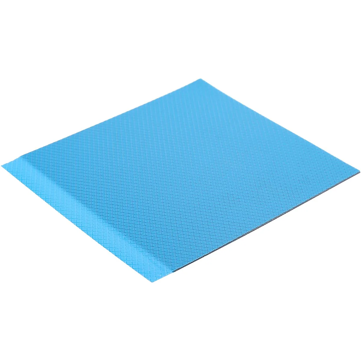
GELID SOLUTIONS GP-Ultimate Thermal Pad 120x120x0.5mm 15W/mK
$13.99
0.00016715BTC
In stockWe take cryptocurrency — so the coins you hold can buy real hardware.Pay in crypto, spend it on real hardware. Free insured shipping worldwide over $399. Plain, unbranded boxes, sent from Germany.Free insured shipping over $399. Your rate is locked for 30 minutes once checkout opens.Rate locked 30 minutes. Every item sealed, serial-checked and covered by a 24-month warranty.Sealed, 24-month warranty.


GELID SOLUTIONS
A 120×120×3.0 mm thermal pad with 15 W/mK conductivity for GPU VRM, memory ICs and M.2 SSDs, non-conductive and rated –60 °C to 220 °C
Option 120 x 120 x 3.0 mm
The GP-Ultimate thermal pad delivers 15W/mK conductivity to bridge uneven surfaces between SMD components and heatsinks. It targets VRM circuits, memory ICs, power MOSFETs and M.2 SSDs where height differences rule out thin paste. The non-electrically conductive, non-corrosive compound stays pliable from -60°C to 220°C without curing or hardening. A single 120×120mm sheet covers enlarged PCB areas in one placement.
The enhanced multilayer matrix maintains its thermal path during prolonged high-temperature operation without pumping out or drying. Non-curing behaviour means the interface remains consistent across repeated thermal cycles from idle to full load. Non-toxic composition eliminates contamination risk on dense component clusters over the product lifetime. The 3.0mm thickness accommodates larger stack-height variances while preserving full-surface contact.
Builders replacing thermal paste on VRM heatsinks, GPU memory banks or M.2 drive controllers gain uniform coverage without air gaps. The jump is worth it when component heights vary across a single heatsink or when rework demands a clean, reusable interface. Thinner 0.5, 1.0, 1.5 and 2.0mm variants exist for tighter clearances, but this 3.0mm option suits the tallest gaps. It does not suit applications needing sub-millimetre bond lines or adhesive mounting.
No published specifications for this item yet.
Other versions of this model
Same family, different memory, cooler or clock — compare before you commit.
It is non-hardening and non-curing, so the material remains compliant across the full -60 °C to 220 °C operating range without stiffening over time.
A flat mounting area on the PCB — such as VRM heatsinks, memory modules or M.2 SSD — large enough to accommodate the full 120 mm square.
Yes, the 3.0 mm profile is designed for height differences and uneven surfaces like VRM ICs and power MOSFETs on legacy boards.
New to this? Which coin should you pay with — what to check, what it costs to pay, and what is never asked for.
Also in this aisle
Same shelf, same checkout — eight coins and a 30-minute rate lock.
What you pay in, and what you read prices in.
Sent from your wallet at checkout
Display only — the catalogue is priced in USD
No currency matches that.
Pick the language the site speaks to you in.
No language matches that.
New here?
Already have one?
There is no automatic reset: this shop sends no mail, so there is no one-time link to ask for. Leave the address on the account and it gets picked up by hand.
Request noted
Nothing is on its way to your inbox — this shop sends no mail at all. Someone picks these up by hand.
Remembered it?