

Knox Gear, Inc.
Knox Gear KN-GC02 39" Hard Shell Guitar Case Gold Hardware
- Guitar Bag
$62.99
0.00075008BTC
In stockWe take cryptocurrency — so the coins you hold can buy real hardware.Pay in crypto, spend it on real hardware. Free insured shipping worldwide over $399. Plain, unbranded boxes, sent from Germany.Free insured shipping over $399. Your rate is locked for 30 minutes once checkout opens.Rate locked 30 minutes. Every item sealed, serial-checked and covered by a 24-month warranty.Sealed, 24-month warranty.

Graviton
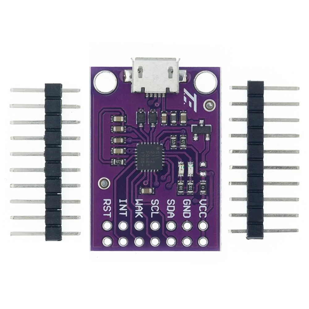
USB-to-SMBus bridge board with CP2112 controller for I²C sensor development and debugging
The Graviton CP2112 debug board converts a USB 2.0 full-speed link into an SMBus or I²C master interface for sensor evaluation. It integrates a USB transceiver, oscillator and eight GPIO pins so developers can communicate with target devices without writing custom firmware. The on-board 194-byte OTP ROM stores product identifiers, while a 512-byte buffer handles SMBus traffic at configurable clock rates.
Verify that the development machine provides a standard USB 2.0 port capable of supplying 4.0 to 5.25 V for bus-powered operation or 3.0 to 3.6 V if the board is self-powered. Ensure the target sensor or peripheral operates with an I/O voltage between 1.8 V and the selected VDD level. The module functions across a -40 °C to 85 °C ambient range, so confirm the test environment stays within those limits.
The board draws power directly from the USB connection and presents a standard HID-class interface to Windows, Mac and Linux hosts, freeing the developer from driver development. Its on-chip 3.45 V regulator supplies local logic, while the eight GPIO pins remain available for additional control or monitoring tasks. Buyers who need a second simultaneous USB-to-I²C channel or a different bridge controller will need a separate solution.
No published specifications for this item yet.
The board is supplied as a standalone module with a Micro-USB 2.0 connector. A Micro-USB cable and any target I2C or SMBus sensor such as a CCS811 module must be provided separately.
Choose USB bus power when a 4.0 to 5.25 V USB port is available; choose self-powered mode when a 3.0 to 3.6 V external supply is preferred. Both modes share the same on-board 3.45 V regulator and 1.8 V to VDD I/O range.
The 12 Mbps USB link feeds a 512-byte SMBus buffer with configurable clock speed, so sustained I2C transfer rates are limited by the SMBus clock setting and 194-byte OTP storage rather than the USB bandwidth.
Also in this aisle
Same shelf, same checkout — eight coins and a 30-minute rate lock.
What you pay in, and what you read prices in.
Sent from your wallet at checkout
Display only — the catalogue is priced in USD
No currency matches that.
Pick the language the site speaks to you in.
No language matches that.
New here?
Already have one?
There is no automatic reset: this shop sends no mail, so there is no one-time link to ask for. Leave the address on the account and it gets picked up by hand.
Request noted
Nothing is on its way to your inbox — this shop sends no mail at all. Someone picks these up by hand.
Remembered it?


